Large Diameter Substrates and SiC Chipsets: Key Developments Shaping the Silicon Wafer Industry
22 Apr
2025
Highlights:
- Introduction
- Latest advancements in the silicon wafer industry
- Product launches in the sector
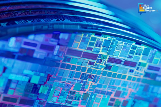
The exponential rise in the use of electronic devices and digital technologies has revolutionized the semiconductor sector in the last few years. The growing use of different kinds of transistors, diodes, and chipsets has led to a surge in the demand for silicon wafers, a key component of modern integrated circuits. Silicon wafers are thin slices of pure crystalline silicon that act as a substrate for microelectronic devices during the process of semiconductor fabrication. Almost all electronic products, ranging from smartphones and televisions to medical equipment and solar panels, feature ICs and chipsets made using silicon wafers. Furthermore, advancements in telecommunication techniques have expanded the scope of this raw material. The launch of 5G technology, for instance, in various developed and developing countries has positively impacted the silicon wafer industry in recent times.
Novel trends in manufacturing and material sciences accelerating sectoral demand
The increasing demand for miniature electronic devices has led to changes in semiconductor fabrication processes and techniques. Companies across the world have started adopting new manufacturing approaches to realign their businesses as per the evolving industry dynamics. For example, the shift toward larger wafer sizes has helped businesses increase the number of ICs per wafer, thus creating more powerful chipsets. Moreover, the use of substrates with large diameters, like 450 mm, aids in improving production efficiency, resource optimization, and cutting down manufacturing costs.
At the same time, technological advancements in the field of materials science have led to the development of new compounds that are better suited for high-power and high-frequency applications. The advent of silicon carbide wafers has enabled companies to address the demand of the renewable energy and power electronics industries, wherein the reliability and durability of the devices are of utmost importance. Compared to traditional ICs, chipsets made from SiC substrates allow for faster switching, thus aiding in faster conversion and low energy losses. Furthermore, the high breakdown voltage offered by this novel material makes it ideal for harsh weather conditions and extreme temperatures.
Increased competition between technology companies opening new investment avenues
The silicon wafer industry accounted for $15.4 billion in 2022 and is predicted to rise at a CAGR of 5.4% during 2023-2032, thus gathering a revenue of $25.9 billion by 2032. Over the years, several multinational technology giants have launched cutting-edge products in the market to gain a competitive edge over their peers and strengthen their position in the industry. For instance, in April 2024, LONGi Green Energy Technology Co., Ltd., a major player in the solar power sector, introduced a new line of TaiRay silicon wafer products, specifically designed for photovoltaic applications. These systems offer full-platform support, enhanced gettering performance, and high resistivity concentration, thereby increasing their utility in modern solar panels. The press release issued by the company highlighted that these products were unveiled after the completion of a long series of R&D tests and system patent layout, thereby making them one of the most advanced solutions in the industry.
Similarly, in October 2024, Infineon Technologies AG, Germany’s largest semiconductor manufacturer, announced the launch of the world’s thinnest silicon power wafer. With a thickness of 20 micrometers and a diameter of 300 millimeters, this new product is expected to create numerous growth opportunities for the consumer electronics sector in the coming period. The wafer has been designed for energy-efficient power solutions, making it an ideal candidate for AI-based applications.
In summary, the rising use of digital gadgets and telecommunication technologies has boosted the revenue share of the silicon wafer market significantly. Furthermore, improvements in manufacturing processes and the emergence of advanced materials are estimated to increase the footprint of the sector globally.
Get in touch with our experts for valuable insights on the growth drivers and investment opportunities in the industry!

Akhilesh Prabhugaonkar
Author's Bio- Akhilesh Prabhugaonkar holds a bachelor’s degree in Electronics Engineering from the reputed Vishwakarma Institute of Technology. He has a special interest in the fields of forensics, world history, international relations and foreign policy, sports, agriculture, astronomy, security, and oceanography. An ardent bibliophile and melophile, Akhilesh loves to write on topics of his interest and various other societal issues. This love for writing made him enter the professional world of content writing and pursue his career in this direction.
Avenue: Entire Library membership of Allied Market Research Reports at your disposal
- Avenue is an innovative subscription-based online report database.
- Avail an online access to the entire library of syndicated reports on more than 2,000 niche industries and company profiles on more than 12,000 firms across 11 domains.
- A cost-effective model tailored for entrepreneurs, investors, and students & researchers at universities.
- Request customizations, suggest new reports, and avail analyst support as per your requirements.
- Get an access to the library of reports at any time from any device and anywhere.
Related Post
Share on Social Media


-
How are Submarine Cables Transforming Global Connectivity with Enhanced User Experience?
-
Endoscopy Procedures: Transformations in Techniques and Applications
-
AI-Powered Video Analytics: How the Product Actually Works for enterprises
-
Painting Robots: Transforming Precision Coating and Creative Applications
-
Innovations in Pharmacovigilance Systems Advancing Patient Safety
-
Understanding Edge Security: Keeping Data Safe Near the Source
-
Exploring the Use and Advancements of 3D Laser Scanners in Professional Applications
-
Reinforcing Industrial Controls with Smarter Tools and Training